AMD Unveils Instinct MI455X: A New Era of AI Acceleration Focused on System-Level Efficiency and Scale

AMD has officially pulled back the curtain on its latest and most formidable AI accelerator, the Instinct MI455X, at the highly anticipated AMD Advancing AI conference in San Francisco. This cutting-edge GPU, boasting an astounding 320 billion transistors fabricated on a 2-nanometer process, is equipped with 432 GB of HBM4 memory and capable of delivering up to 40 petaflops of FP4 compute power. However, the narrative surrounding this generation of Instinct accelerators transcends mere brute force, shifting instead towards a profound emphasis on efficiency and the integral role of the GPU within a larger, interconnected system.
"The goal is no longer to build the biggest GPU. Although we have built a pretty big one," quipped Alan Smith, Corporate Fellow and lead architect for the Instinct line, during the technical briefing. This statement underscores a strategic pivot within AMD, acknowledging that the escalating demands of modern artificial intelligence workloads necessitate a more holistic approach to hardware design. The focus has decisively moved from individual component prowess to optimizing the entire computational ecosystem. Smith elaborated, "The goal is to build a system that aligns with the communication and execution patterns of AI workloads. Models and infrastructure evolve together; the next leap in AI performance comes from the co-design of both as a single entity." Consequently, the MI455X is not presented as a standalone marvel but as an inseparable component of AMD Helios, a rack-scale system designed to integrate 72 of these powerful GPUs into a single, cohesive supercomputing unit.
A Deep Dive into the CDNA 5 Architecture on 2 Nanometers

The Instinct MI455X is engineered upon the novel CDNA 5 architecture, marking it as one of the pioneering chips to leverage TSMC’s advanced 2-nanometer manufacturing process. This represents a significant leap in semiconductor technology, promising unprecedented transistor density, improved power efficiency, and enhanced performance. Retaining AMD’s proven chiplet design philosophy, the MI455X introduces a revamped layout for optimal AI acceleration. The core computational power resides in eight Accelerator Complex Dies (XCDs), meticulously produced on the 2nm process, collectively housing 256 active workgroup processors.
A pivotal innovation in this generation is the introduction of two dedicated Fabric-and-Cache Dies (FCDs), fabricated on TSMC’s N3P process. These FCDs are crucial, as they host the revamped L2 cache—now structured as two blocks of 96 MB, each shared by eight shader engines. This architectural shift significantly enhances data accessibility and throughput. Complementing these are two I/O dies, with the entire intricate assembly packaged using CoWoS-L (Chip-on-Wafer-on-Substrate-L) technology and 3D hybrid bonding. These advanced packaging techniques are vital for integrating diverse chiplets while maintaining high bandwidth and signal integrity. This re-architected cache and packaging strategy delivers a substantial threefold increase in cache bandwidth compared to the Infinity Cache of its predecessor, the MI355X, and up to a fourfold bandwidth amplification by employing multicast to send tensor data to multiple compute units simultaneously.
Furthermore, the CDNA 5 architecture fundamentally shifts to native Wave32 execution, a paradigm previously seen in AMD’s RDNA consumer graphics cards, while definitively moving away from Wave64. In practical terms, where a single instruction previously required four cycles to traverse a 16-lane wide SIMD unit, the MI455X can initiate a new instruction every cycle on a 32-lane wide unit. This enhancement drastically reduces instruction latency and mitigates the performance penalties associated with branching code, a common occurrence in complex AI models. The chip also fully supports the Open Compute Project (OCP) MX standard for block-scaled data formats, including fractional scaling. This capability is instrumental in making FP4 (4-bit floating point) training practically viable by effectively minimizing quantization errors, thereby accelerating training times and reducing memory footprint for large models.
Unpacking the Performance Metrics and Efficiency Imperatives

The specifications of the Instinct MI455X paint a compelling picture of its capabilities:
| Specification | Instinct MI455X | Compared to Instinct MI355X |
|---|---|---|
| Process Node | 2 nm (TSMC), chiplets | — |
| Transistors | 320 billion | — |
| Memory | 432 GB HBM4 (12 stacks) | Up to 1.5x more |
| Memory Bandwidth | 23.3 TB/s | Up to 2.9x more |
| Peak MXFP4 | 40.26 petaflops | Up to 4x more |
| Peak MXFP8/FP8 | 20.13 petaflops | Up to 4x more |
| Peak MXFP6 | 20.13 petaflops | Up to 2x more |
| Matrix FP16/BF16 | 5.03 petaflops | Up to 2x more |
| L2 Cache | 2x 96 MB globally shared | New cache hierarchy |
| Scale-up Bandwidth | 3.6 TB/s per GPU (UALoE) | — |
These formidable specifications translate into significant real-world advantages. AMD claims the MI455X can deliver up to 34 times greater token throughput and up to 18 times lower cost per token compared to the Instinct MI355X, based on measurements taken using DeepSeek V4 Flash with FP4 precision. A crucial detail emphasized by Anush Elangovan, AMD’s Senior Vice President for Software, during the briefing was that these core figures—specifically, 20 petaflops of FP4 performance and 20 TB/s of HBM bandwidth—are not mere projections but measured values from operational hardware in AMD’s laboratories, lending substantial credibility to the performance claims.
Beyond raw computational muscle, AMD’s strategy prioritizes efficiency and intelligent resource utilization. "We must simultaneously optimize for compute, memory, communication, energy efficiency, and cost," stated Alan Smith. To this end, the MI455X integrates an array of sophisticated techniques. A new Tensor Data Mover intelligently overlaps memory transfers with computation, ensuring continuous data flow to the processing units. Workgroup clusters provide programmers with fine-grained control over data placement, enabling highly optimized memory access patterns. Split barriers facilitate more efficient synchronization across parallel tasks, reducing overhead. Furthermore, significantly lower kernel-start latency ensures that even short-duration kernels can keep the machine fully utilized, maximizing overall throughput.
The Direct Memory Access (DMA) architecture has been completely re-engineered to automatically distribute data transfers across available connections, intelligently factoring in network congestion. Closer to the compute cores, capabilities have been scaled to meet the escalating demands of modern AI models. The local datastore per workgroup processor has doubled in both capacity and bandwidth, and individual threads can now access up to 1,024 registers, a substantial increase from the previous 256. This expanded register file is essential for effectively feeding the wider vector units and handling the complex state required by advanced AI algorithms.

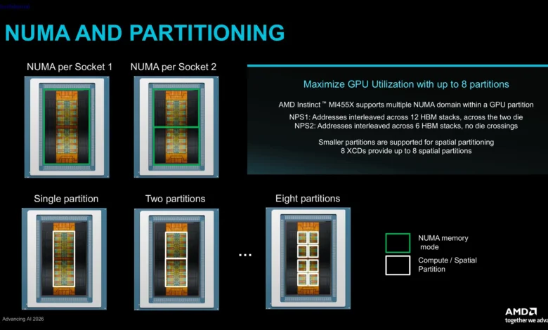
The MI455X also offers remarkable flexibility through various NUMA (Non-Uniform Memory Access) modes. The GPU can operate as a single, expansive memory domain, be logically split into two, or even be partitioned into up to eight smaller virtual GPUs for virtualized environments. This capability is vital for cloud service providers and large enterprises seeking to efficiently allocate and isolate resources for multi-tenant AI workloads. Security is a paramount concern, and the MI455X scales robust hardware-level protection from the chip to the rack. A hardware-rooted trust mechanism and confidential computing capabilities safeguard model weights, prompts, and KV-caches during execution. Within the AMD Helios system, virtual pods ensure complete isolation between different tenants, addressing critical data privacy and intellectual property concerns in shared infrastructure.
Two Flavors: MI455X and MI430X Tailored for Diverse Needs
The MI400 series launches with two distinct members, each meticulously designed for specific target audiences:
| Instinct MI455X | Instinct MI430X | |
|---|---|---|
| Target Group | Frontier-AI and AI-factories | Sovereign AI and HPC |
| Deployment | AMD Helios rack-scale (72 GPUs/rack) | Classic mesh-based HPC clusters |
| Strength | Up to 40 PF FP4, maximum token throughput | Up to 288 TFLOPS hardware FP64 |
| Memory | 432 GB HBM4 | HBM4 |
The Instinct MI430X showcases AMD’s enduring commitment to high-performance computing (HPC), a segment where it has historically maintained a strong presence. While many competitors have largely de-emphasized hardware-accelerated FP64 (double precision) compute in favor of AI-centric precisions, AMD, leveraging its flexible chiplet approach, combines robust FP4 AI compute with full-fledged double-precision capabilities. This unique blend makes the MI430X an ideal solution for research institutions and national labs that require a single infrastructure to handle both cutting-edge AI training and traditional scientific simulation workloads, addressing the growing convergence of AI and HPC.

AMD Helios: The Engine of Rack-Scale AI Supercomputing
The Instinct MI455X is explicitly designed as the foundational engine for AMD Helios, a rack-scale system launched concurrently with the new GPU. Helios represents AMD’s vision for a fully integrated, high-performance AI supercomputing platform. Within this system, 72 MI455X GPUs work in concert, with groups of four GPUs paired with a single AMD Epyc Venice SP7 processor. These Epyc processors, based on the Zen 6 architecture, integrate into the memory domain via coherent Infinity Fabric, providing a staggering 256 GB/s bandwidth per GPU. This tight integration means the CPU acts not merely as a PCIe host but participates directly in a unified memory architecture, greatly reducing data movement bottlenecks.
Each MI455X GPU in the Helios system features 3.6 TB/s of scale-up bandwidth through UALink over Ethernet and accommodates three 800G network cards for scale-out connectivity. This intricate network topology ensures extremely low latency and high bandwidth communication both within and between nodes. The cumulative effect is a single rack capable of housing 31 TB of HBM4 memory, delivering an astonishing 2.9 exaflops of FP4 compute power, and boasting an internal bandwidth of 260 TB/s. A critical design feature of Helios is that every GPU can reach every other GPU in the rack in a single hop, minimizing communication overhead and maximizing the efficiency of distributed AI model training and inference.
Navigating the Competitive AI Landscape: AMD vs. NVIDIA

Naturally, the benchmark for the MI455X and Helios is NVIDIA’s Vera Rubin NVL72, a formidable competitor unveiled at CES and also slated for release in the second half of the year. On paper, AMD asserts a competitive edge, claiming 15 percent more FP4 compute, 50 percent more HBM memory, and up to 30 percent lower cost per token compared to NVIDIA’s offering. In terms of scale-up bandwidth, both racks appear to achieve parity with 260 TB/s.
However, such comparisons warrant careful consideration. AMD’s claims are based on its own measurements and internal models, pitted against the publicly released specifications of a system (NVIDIA’s) that has yet to reach customer deployment. Conversely, NVIDIA has promised up to five times the inference performance of its Blackwell architecture and ten times lower token costs in its own projections. As is often the case in the rapidly evolving semiconductor industry, "paper is patient" on both sides, and real-world performance will be the ultimate arbiter.
Crucially, NVIDIA’s most enduring competitive moat remains its software ecosystem, particularly CUDA. While AMD’s top software executive, Andrew Dieckmann, may dismiss CUDA as a "non-event" during the briefing, this statement inadvertently highlights AMD’s most significant hurdle. The vast majority of AI tooling, extensive documentation, and the established developer community are deeply entrenched in NVIDIA’s ecosystem. The Vera Rubin architecture, when it ships, will integrate seamlessly into a customer base already familiar with and heavily invested in NVIDIA’s Blackwell and prior generations. AMD has made significant strides with its ROCm open-source software platform, but building a comparable ecosystem takes sustained effort and time.
AMD itself acknowledges that comparisons between GPU vendors often represent fleeting snapshots of who has the most advanced software stack at a given moment. This truth cuts both ways; AMD’s current advantages could be quickly eroded if NVIDIA updates its software stack or introduces new architectural optimizations.

Strategic Implications and Future Outlook
Despite the formidable challenge posed by NVIDIA’s dominance, AMD’s advancements with the MI455X and Helios carry profound strategic implications for the AI industry. The consistent roadmap, with the MI500 series slated for 2027 featuring next-generation HBM and an expanded scale-up domain utilizing both copper and optical interconnects, followed by the MI600 already in development, signals AMD’s unwavering long-term commitment to the AI accelerator market.
Perhaps the most compelling indicator of AMD’s growing traction is the list of major customers now deploying its AI solutions. With industry titans like OpenAI, Meta, Anthropic, Microsoft, and Oracle committing to integrate AMD’s offerings, gigawatts of NVIDIA-alternative compute are being brought online for the first time. This diversification of supply is critical for the healthy growth of the AI industry, fostering competition, potentially lowering costs, and accelerating innovation.
The MI455X is not merely tasked with outperforming Vera Rubin on every metric; its more fundamental mission is to prove that AMD has matured into a fully viable and robust second supplier in the high-stakes AI accelerator market. On paper, the evidence for this maturity has been compellingly presented. The true test, however, will unfold in the second half of the year, as these advanced systems are deployed and begin operationalizing the next generation of AI in real-world data centers across the globe.
Related posts: